< Previous | Contents | Next >
| G: Hardware Projects |  |
|
CLOCK add on
For under £2.00 some 512 users can extract a 20% speed improvement from their 512 board. However, be aware that there are potential problems and success is not guaranteed. The practicalities are simple and if you are competent with a soldering iron this modification can easily be tried and more importantly, reversed if it fails.
All that is required is to remove the 512 board from your machine, desolder the 20Mhz crystal (X1) and replace it with a 24Mhz crystal. These are obtainable from any decent electronics component supplier.
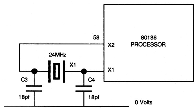 |
| Figure 1 - Clock Circuit |
The crystal is the silver metal-cased component located immediately at the side of the processor chip. It is soldered into the 512 board by two connections only.
By changing the crystal for a faster one you will be running the 80186 at 12MHz instead of 10Mhz. This works with some 80186 processors, but as it means running the processor 20% over its rated speed it is not reliable in all 512s. The only way to know is to change the crystal and test your 512 at 12Mhz. You will soon know if it doesn't like working out of specification – it won't boot correctly, or will crash out with random spontaneous errors within a few hours of being turned on. If this happens you might find that increased cooling (if possible) will relieve the problem. (Running the processor faster than its rated performance for a few hours is most unlikely to cause any damage, even if it ultimately does not succeed.)
In addition to the processor chip itself, another cause for the faster 512 failing may be the external co-processor box. This can occur with either a Master or a BBC B/B+. The usual problem is timing, but it does work for some systems and Robin Burton has been running his 512 at 12 Mhz in an external co-pro attached to a model B for some time now without difficulty. If you do have problems, but really want to persist with this experiment the only other thing to try is replacing the 80186-processor chip itself.
Intel have now superseded the 80186 with the CMOS 80C186 which is a faster processor, but which is fully compatible and can be used as a direct replacement for the standard 80186. The 80C186 is available in 10 Mhz, 12 MHz and 16 Mhz versions.
You can replace the 80186 with a 12 MHz 80C186 (and this time you must change the crystal for a 24Mhz version) to get the 20% performance increase.
If you are really keen on modffications and hardware projects, you can try changing the 80186 for a 16Mhz 80C186 using a 32Mhz crystal, but be warned that you will certainly need to change both the two EPROMS and possibly the RAM too, since these would otherwise operate too slowly. This modification is clearly much more ambitious and costly than the change to 12Mhz, but it certainly would produce an extremely fast 512!
NB: It is not possible to change the 80186 for any vession of 80286 or 80386, because these processors are not pin compatible. It would therefore require extensive modifications to both the 512 board and to the software. You should also be aware that you would receive no benefit unless you used a fast 286 or 386, which cost very much more than a 186!
Master 512 RAM expansion board
This is a hardware project for those who would like more memory in their Master 512 and are handy with a soldering iron. The aim is to add a second bank of 512k of RAM to the 512 board, giving 1024k in a similar manner to the Solidisk PC+.
Publisher's note: You are advised not to attempt this project if you have no previous experience of circuit hoard construction and soldering, no matter how experienced you may be in other areas of using or programming the 512. Also note that incorrect assembly or fitting could feasibly damage the 512. This is not a beginner's project, nor are the costs trivial. As a rough guide, at the time of going to press raw materials costs are likely to be between £40 and £50 and RAM costs are currently increasing rapidly. If you do not feel completely confident about your abilities you are advised to refer to Appendix H for details of commercially produced 512 memory expansion boards. Dabs Press are unable to advise or assist in the building of this project.
Every effort has been made to ensure the accuracy of this design and successful prototypes have been built. However, the publisher, the author and the circuit designer accept no liability for any consequences arising from the use of this information, nor can they offer a consultancy service to anyone who encounters difficulty as a result of attempting the project. Use of the design is limited to the personal needs of the reader, this design may not be used for commercial purposes. Full acceptance of these terms and limitations is implicit in the use of this circuit design and its construction details.
Materials you will need:
Qty |
Item |
||
| 16 | 256kx1 150ns DRAMs | ||
| 1 | 74LS75 | ||
| 1 | 74LS139 | ||
| 1 | 74LS08 | ||
| 6 | 47nf decoupling capacitors | ||
| 1 | 10μf electrolytic capacitor | ||
| 3 | 2.2kΩ resistors | ||
| 2 | Extended leg (15mm) 28-pin sockets | ||
| 16 | 16-pin sockets (if you wish to socket your RAM) | ||
| 1 | Piece of vero board (wire wrap type) size 120 mm x 120 mm | ||
| 1 | Reel of 0.2 mm insulated wire | ||
| 1 | Reel of 0.5 mm insulated wire | ||
| or | Wirewrapping tools |
If you wish to socket the 74LS chips add two more 16 pin sockets and one 14-pin socket to the list.
The Master 512 uses 16 256k x 1 DRAMs. These are split into 2 banks of 256k bytes – the high byte and the low byte forming the 16-bit word used by the 80186. Each RAM bank holds one bit of each byte, hence 1 byte of each word. By adding a second bank of 512k wired to give the same format, you can have 1024k bytes of RAM.
The first task is to physically set out the RAM chips on the board. This is done using a similar layout to the RAM on the 512 board. Set out two banks of 8 chips, one as the high byte, the other as the low byte.
The next thing to consider is supplying the address and data lines to the RAM. On the 512 board the RAM, the processor and the ROMs have access to both the address and the data lines. To avoid too much soldering on the 512 board we can use the address and data lines from the EPROMs, especially as these are socketed. The address lines to the EPROMs are already split into high and low bytes, so this is highly convenient. The other signals that must be supplied are RAM read/write and refresh, the Row Address Strobe and Column Address Strobe. These are labelled RAS and CAS respectively on the diagrams.
The RAS and CAS are generated on the 512 board for its own RAM and we must patch into these signals for our extra RAM. We will need to supply address lines 18 and 19 (A18, A19) separately, as these are used by the EPROMs to decode the high bank.
The last thing the RAM requires is power. This is usually 5 volts on Vcc and ground (0 volts) on Vss. Power must be supplied to the addressing chips and can most conveniently be taken from the 512 board. As we are taking most of our signals from the EPROMs, we can conveniently take the power from there too.
Important: All chips and sockets have a notch at one end. This is the 'top', also commonly called 'north' on circuit diagrams. Chips must be connected the correct way round. If they are not, not only will they certainly not work, but they may be damaged, and might well cause damage to other chips in the circuit when power is applied.
Pin 1 (for all chips) is always at the top left corner, next to the notch when the chip is viewed from above (ie the opposite side to where the legs point) with the notch at the top. Pin 2 is the second pin down on the left side and so on down to pin 8 for the RAM chips and the two 16 pin 74LS chips, 1 to 7 for the 74LS08 and pins 1 to 14 for the two EPROMs. Numbering then continues on the right side of the chip, but from the bottom upwards towards the notch this time. The pin assignments are also shown on the diagram.
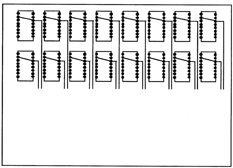
Now to start laying out the board, beginning with the RAM (you can use sockets if you prefer not to solder chips directly). The first thing is to place the RAM chips (or their sockets) on the Veroboard. Lay them out as two banks of eight positioned about one hole apart and with pin 1 to the top. Solder each corner to hold them in. Your layout should be similar to this:
 |
| Figure 2 - RAM Bank Layout |
The pin out of the RAMs is as follows. For each bank of RAM we need to join the address lines together along the banks, bringing the lines out of the left hand end of the banks.
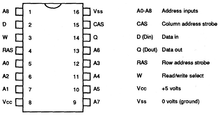 |
| Figure 3 - Pinout of DRAM |
For each of the two banks, using the underside of the board, join A0 (pin 5) on chip 1 to A0 on chip 2 to A0 on chip 3 and so on right down to chip 8. Do the same with all the other address lines, ending with A8. Extend the address lines (A0 to A8) so that they come out of the left hand side of the two banks, but don't join the banks up yet.
Each bank should now look like this:
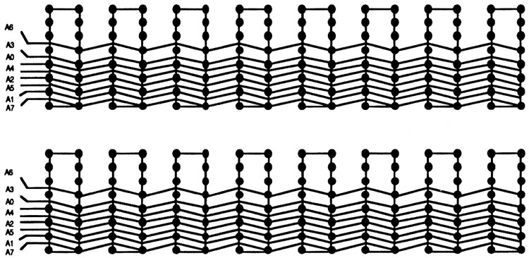 |
| Figure 4 - RAM Address line Connections |
The other lines, that is W, RAS and CAS should now be joined chip to chip in a sirnilar fashion. That is for each bank, join the appropriate pin of each chip to the sarne pin of the next chip, through all 8 chips. With these lines however, extend them out of the right hand side of the banks.
This just leaves power, Data in (D) and Data out (Q) unconnected.
On each chip join Data in to Data out. Now using the topside of the board, extend the data line for each RAM chip down between the chips, to the centre of the board.
 |
| Figure 5 - Data Line Connections |
Put the two EPROM holders onto the vero board with pin 1 to the right <?>. Place them so that they plug directly into the EPROM sockets on the 512 board, leaving the RAM 5mm clear of the processor. Next, solder the four corners of the sockets to the vero board. On the 512 board, IC31 is the low byte, and IC32 is the high byte. Using the top one of our two RAM banks as the high byte, join the data line of RAM 1 to D0 on the IC32 EPROM socket, then the data line of RAM 2 to D1 on the IC32 EPROM socket, and so on until you have the data lines on each RAM joined to the relevant data line on the EPROM socket. The top RAMs should be joined to D0-D7 on IC32 and the bottom RAMs should be joined to D0-D7 on IC31.
 |
| Figure 6 - EPROM pinouts |
Now on the underside of the board, do the same thing for the address lines. For the top bank join the address lines to the corresponding address line on IC32. Then do the same for the bottom bank, joining the address lines to IC31.
Next we must add the control lines. The CAS is quite easy and is just a matter of connecting the CAS signal generated on IC6, pin 8 on the 512 board to the CAS inputs of the RAMs. The RAS however must be patched in such a way that it does not interfere with the RAS signal on the 512 board.
As on the 512 board, we need separate strobes for the high and low bytes. These can be derived from the RAS signals provided by the 512 board. It is done using a 2 to 4 line decoder, in this case a 74LS139. This should be added onto the expansion board at the right hand end.
We also need two 2 input AND gates to combine the outputs of the 74LS139 and the 74LS113 on the main board. These are supplied by the 74LS08. The connections are described below and are also shown on the circuit diagram.
The best way to connect the RAS signals from pins 6 and 8 of IC 4 on the 512 board to our extension board is to desolder pins 2 and 4 of IC6 on the 512 and lift them from the board. Next solder the following:
| 1. | A flylead from pin 2 of IC6 to pin 12 of the 74LS139 |
|
| 2. | A flyIead frorn pin 4 of IC6 to pin 4 of the 74LS139 |
|
| 3. | A flylead from the vacated pad of pin 2 of IC6 to pin 14 of the 74LS139 |
|
| 4. | A flylead from the vacated pad of pin 4 of IC6 to pin 2 of the 74LS139 |
The next part is easier, as the 74LS08, IC6 is next to the edge of the board and so is easier to work on. IC6 pins 2 and 4 are two of the inputs to the AND gates on the main board. On the 74LS139, join pin 13 to pin 3 so that the same signal can be used to supply both inputs. Also join together pins 1, 8 and 15, this grounds the enable pins for both decoders. Pin 8 will eventually also be joined to the earth rail.
We now need to fit the last two ICs to the expansion board. These are a 74LS08 positive AND gate with totem-pole output, and a 74LS75 4-bit bi-stable latch. These should be fitted near the 74LS139.
Join pin 3 of the 74LS139 to pin 15 of the 74LS75. This allows the Q output of the 74LS75 to drive the B inputs on the 74LS139. Now to add a few more fly leads. The first needs to go from IC3 pin 4 on the 512 board to pin 4 on the 74LS75, then also join pin 4 to pin 13 on the 74LS75. This supplies the enable signals to the 74LS75.
Now to fit the fly leads from the processor. You may alternatively remove the processor from its socket and solder onto the socket, or you can solder directly to the processor. Both methods work, but for safety you are strongly advised to carefully remove the processor chip and solder to the socket. Small cut outs are provided at opposite corners of the 80186's socket to allow insertion of fine screwdrivers, probes etc to allow removal of the chip. Insert your chosen tools and lever the chip out evenly. Take great care, the 80186 processor is expensive to replace if damaged.
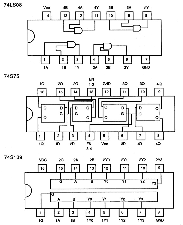 |
| Figure 7 - Pinouts for 74LS08, 74LS75, 74LS139 |
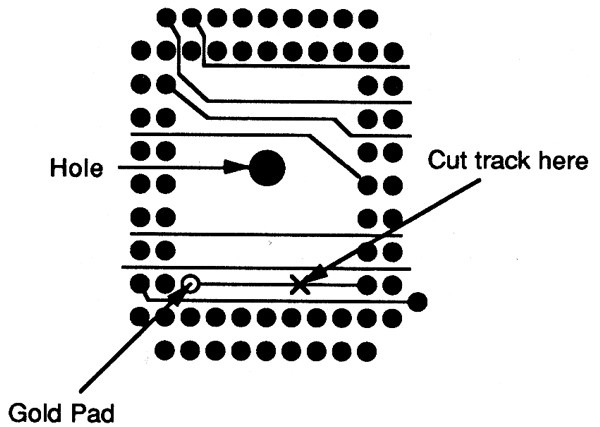 |
| Figure 8 - Cutting the Master 512 tracks |
The first signal required is the "not lower chip select" from pin 33 of the processor. We also need to cut the track between pin 33 of the processor and the through-plating, effectively disconnecting this pin from the main board. Turn the 512 board over, and place it so that the main board connectors are to the left and right, and the sticker showing the serial number is near the top of the board (away from you). Locate the processor, a square of connections, two pins deep all around. You will see a gold pad at the bottom left, inside the processor connection. A track leads from this pad, horizontally across to a processor pin. This should be cut through with a sharp knife taking great care not to damage any other track in the area. Now connect a fly-lead from pin 16 of the 74LS75 to the through plating on the main board so that we are supplying not-LCS instead of the processor. The other two signals required are A18 and A19. These require a fly-lead from pin 2 of the 74LS75 to pin 65 of the processor and a fly-lead from pin 3 of the 74LS75 to pin 66 of the processor.
Now for the 74LS08. On this we are only going to use two of the four AND gates; pins 1, 2 and 3 are the first and pins 4, 5 and 6 are the second. The first two inputs come from the 74LS139 (1Y2 and 2Y2).
Wire pin 10 of the 74LS139 to pin 2 of the 74LS08, then pin 6 of the 74LS139 to pin 5 of the 74LS08 to obtain these signals.
The signals that these are ANDed with come from IC6 pin 5 on the 512 board. They are obtained by wiring a fly lead from pin 5 of IC6 on the 512 board to pin 1 of the 74LS08, then joining pin 1 of the 74LS08 to pin 4.
The outputs of the 74LS08 are the RAS signals for the RAM. These are on pins 3 and 6, but as the signal is a NOT RAS signal the lines need to be pulled high to stop them floating. This is done by pulling these pins up to 5 volts through two 2.2kΩ resistors.
The resistors should be fitted near pins 3 and 6 of the 74LS08 with room between the resistor and the pin to take off another lead. The pin should be joined to one end of the resistor and the other end of the resistor should be joined to the +5V rail. The RAS line that you wired in for the low byte on the RAM should then lie joined between pin 3 and the resistor, and the RAS for the high byte should be joined between pin 6 and its resistor. This gives us the row address strobe for both banks of RAM.
For the CAS we need to take this from the CAS signal on the 512 board. This is done simply by wiring both the high byte and low byte CAS lines on the RAM board together and fixing them to one point, then taking a fly lead from this point to resistor R9 on the 512 board.
Attach the fly lead to the end of the resistor nearest to the edge of the 512 board (to the left of IC6). Again this is an active low signal, so needs to be held high. This is done by wiring a 2.2kΩ resistor from the point where the fly lead and CAS lines join to the + 5V rail.
Next we will join in the NOT write signal by yet another fly lead. Again we are going to join the two W signals from the RAM together at a point (or pad) on the RAM board.
From this point we can then take a single fly lead to the 512 board and pick up the W signal from the resistor R11 on the main 512 board. Take the signal from the side opposite IC3.
Last, but equally important, is the power for the RAM chips. This is best provided by adding two power rails that run around the board, one from the +5 volt pin of one EPROM to the +5 volt rail of the other EPROM, and a rail from the 0 volt line of one EPROM to the 0 volt rail of the other EPROM.
Use thicker wire for the power supply rail and try to go as near to the power pins of all the ICs as possible. Join all of the Vcc pins to the +5 volt rail and all of the Vss pins to the 0 volt rail (this pin is sometimes labelled Vdd). Next, to each of the +5 volt connections to the RAM, solder on a 47nf decoupling capacitor to the +5 volt rail, and solder the other end to the 0 volt rail. Repeat this for all 16 RAM chips.
Finally about halfway around the power rails, solder a 10µF electrolytic capacitor across the two power rails, joining them together.
Ensure that you get the capacitor the right way around otherwise it may well go bang. It should have a '+' mark on it. This is the end that should be joined to the +5 volt rail.
Now plug in The EPROMs, the RAM and the ICs (if you used sockets). Plug the RAM board into the 512 board, check all the connections, and then test the unit.
If you have built it correctly, booting up the system using DOS+ 2.1 should give you 768k of free memory.
Building Your Own Hard Disc
It is not the intention of this book to teach electronics, in spite of the 512K memory expansion elsewhere. That was prompted by termination of supplies of the Solidisk PC+. However, there is one other area worth outlining, since it will surely be of interest to many 512 users. We have included it because being aware that something is possible is often half the battle.
A desirable addition to any microcomputer is a Winchester, often called a hard disc. The Master 512, with its much bigger memory, potentially much larger data files and usually much larger application programs makes this an even more attractive proposition. Floppy discs of 640K may be adequate for the BBC micro, even if sometimes inconvenient, but for serious users of the 512 disc capacity, even with the 800K format available in DOS Plus, can be a serious restriction on the use of large applications such as a database or a spreadsheet.
512 users, more than most, are also aware of the fact that hard discs for PC clones are very much less expensive than similar capacity devices for the BBC micro, sometimes as little as half as much. This disparity in cost between ostensibly the same type of device intended to serve the same purpose has led some users to seek an alternative to purchasing a ready made BBC micro hard disc drive.
The differences in cost between a complete hard disc system and the individual components required to make one has induced some enthusiastic users to build their own units from individual boards, though not usually from individual IC components, although this is also possible!
This approach no longer offers such savings as it used to, primarily because the disc cartridge, which used to be the most expensive component, has vastly reduced in price over recent years. This is of course largely due to the increasing popularity of this type of add-on which, perversely for the 512 owner, has occurred mainly because of the IBM PC and its various lookalikes. For example, hard discs of 20 to 30 megabytes which now can be purchased 'ready to go' for about four hundred pounds for the BBC micro and two hundred pounds or so for a PC, could have cost well over £1,000 only two or three years ago.
However, the impetus to save money is still driven by the price of PC hard discs. These are available at under £200 for a 20Mb drive for a PC (and very little more for 30Mb) and understandably BBC Micro users feel hard done by that they must pay double this or more.
The criticism is not entirely fair, as there is one particularly expensive component in the BBC system that is not needed by a PC. The unfortunate fact is that this component remains expensive, because outside of the BBC micro market its use is fairly limited. As you'll see in the following list, this particular component now costs more than the bare disc and drive. Accepting that prices have fallen, even for BBC micro hard disc systems, you can still probably save about £100 by putting the system together yourself.
This is not a difficult job. It certainly requires no electronic skills, and probably (unless a wire falls off) requires little or no soldering either. There is also a certain satisfaction in knowing that you did the job yourself, but as with most 'good ideas' there are cons as well as pros. and this one is no exception. In this case you must remember that there aren't any guarantees on a home-built system. Should it fail, either because of bad workmanship or because you have used cheap or faulty components, you're probably on your own.
The equipment required to run a hard disc on a BBC micro is:
| A SCSI interface card | £175-225 | ||
| A host adaptor card | £35-40 | ||
| A power supply | £10-20 | ||
| A case (optional) | £10-20 | ||
| Cables | £10-15 |
These prices are naturally approximate, but were typical in the summer of 1989. It is assumed that you already have an Acorn compatible ADFS system. If not then this cost must be added.
Many people start their search for the other components after acquiring for little or no cost the hard disc unit itself. Real bargain hunters can probably substantially improve on the prices for the case, power supply and so on, but the two cards required, the host adaptor and the SCSI are going to remain costly items. In fact one of these, the SCSI, virtually on its own accounts for the difference in price between PC and BBC drives. PCs don't need an SCSI interface, BBCs do. You may consider avoiding the SCSI and designing your own direct hard disc connection to the 1MHz connector, but remember that if you do this Acorn's ADFS will not support your hard disc system and you'll also have to write the driver software.
The SCSI Interface
The SCSI (Small Computer Systems Interface) is a standard interface used to transfer data at high speed between micros and various peripheral devices. It is most commonly used (outside Acorn systems) for interfacing laser printers, plotters and scanners, as well as for one-off specialist applications. The 'intelligent' control required at the computer end is limited to issuing high-level commands, usually followed by parameters. For example the ADFS sector read and write commands use codes &08 and &0A, which are in fact the SCSI command codes for reading and writing data.
All SCSI hard disc controller cards are functionally the same, and all of them should have the same connectors on board. The SCSI standard was formerly known as SASI. This was originally developed by Shugart, the pioneer hard disc manufacturer, initially for their own products. Subsequently the standard was adopted as an ANSI (American National Standards Institute) standard, and reissued with slight modification as SCSI. SASI was the acronym for 'Shugart Associates Systems Interface' but this name was unacceptable to ANSI as it included and effectively advertised a trade name, hence the change.
Most SCSI cards will work correctly with the BBC Master. The one manufactured by Adaptec can be specifically recommend as Dabs have had one of these device running on one of their own BBC Masters for over two years without problems. You need not assume that other cards are not as good, but firm recomendations can only be given from our own experiences
The Host Adaptor
The 'host adaptor' card is a simple interface which converts Acorn's 1MHz bus signals to or from the correct format for the SCSI interface. It has connectors for both the SCSI bus and the BBC 1MHz bus. The card is specifically for BBC micros, and therefore normally must be obtained direct from a BBC rnicro dealer. The cards are made by Acorn and a few other suppliers.
Other Components
The remaining components can be obtained either from your local Acorn dealer, a local electronic component dealer or by mail order from one of the many suppliers who advertise from time to time in the BBC micro press. PC magazines are also a source for such dealers, as are some of the electronics hobbyists magazines. Indeed some dealers specialise in hard disc kits or components, and the better ones can usually supply reasonable instructions or diagrams about how to put the components together, as well as supplying sundry items like screws for fixing the finished drive into a case.
If you are able to find a single dealer who can supply most or all of the requisite components you will to some extent minimise the Iikelihood of incompatibilty, and will certainly be better placed to request assistance if you have trouble and suspect faulty components
Having put your hard disc together, the next step is to connect it and test it.
Formatting
There are two stages to preparing a Winchester for use in DOS Plus, the first step being that the Winchester must be formatted in ADFS. 'Ready to go' Winchesters for Acorn systems are often supplied ready formatted, but depending on where you obtained your drive, you may not be so lucky.
The format program needed for Winchesters is not the one used for floppy drives, but it is specific to Acorn machines and so is not a standard DOS program either. The formatting utility should be supplied as part of the the package when you buy a ready made drive for the BBC micro, which of course is of no help whatever if you have built your own, unless components were bought from a dealer specialising in Acorn systems.
The simplest solution is to find someone with a complete drive and to persuade them by fair means or foul to format yours for you, or to allow you to do it on their micro. This is necessary because it would be an infringement of copyright if you were to acquire a free copy of the program yourself from another user. However, some suppliers may be prepared to supply a format program directly.
The Acorn version of the Winchester formatting program is called Superform, which is a BASIC program contained in a directory called FORMAT on the Winchester itself, since Acorn Winchesters are supplied ready formatted.
It is not the intention in this section to explain how Superform works, and in any case you may be using a different program, but there are naturally common elements to formatting a Winchester whatever sofiware you use.
Unless software which is used is written for only one size of drive, the program will require that you supply parameters to indicate the number of tracks and sectors. You should be aware that in some programs default parameters are provided. For example the default Superform parameters will format a 10Mb drive, even if a 20Mb or 30Mb device is being used, in other words there is no automatic sensing of the drive's capacity. To supply the correct values you may need the data sheet for your particular drive. This should accompany the drive when you purchase it.
There are major differences between the processes of formatting Winchesters and floppy discs. One you wlll certainly become aware of is that formatting a Winchester takes longer, and very much longer for the larger sizes like 40 or 60Mb. Also, depending on the format program used, you may see displayed messages indicating the number of bad sectors found on the disc. Although alarming at first sight, this is quite normal because, given the large number of sectors and the high data density of the disc, a limited number of errors is almost unavoidable.
To cater for the loss of storage which would otherwise result from bad sectors Winchesters have a reserved area. Bad sectors or tracks are mapped onto this reserved area during formatting in such a way that references to the bad adresses are re-directed to the reserved area. After formatting is complete your Winchester is ready for use as a large capacity ADFS disc.
To use the Winchester in DOS+ you must then carry out stage two. This is done by booting DOS normally, then using HDISK, included on DOS+ issue disc 1, to create a DOS partition. This is an ADFS file which is recognised by DOS+ as drive C: and it is referred to as such when you access it. If you've previously been using the Winchester in ADFS, as with all disc operations, take sensible precautions. Before you start ensure that you have adequate, up to date backups of all your files.
The size of the partition to be set up is selected during the HDISK initialisation process. This creates a locked ADFS file of the size requested. You can also make the hard disc bootable by copying the system files to it during this process, although this is optional.
The partition size will depend on the size of your Winchester and the amount of space you want in DOS (and ADFS) but ensure that there is enough free space (in ADFS) to allow for the DOS partition, or the initialisation will fail. The remainder of the disc, after the partition is set up, is available for use in ADFS when operating in native BBC mode.
The DOS Partition is allocated as an ADFS file, and it's a good idea to force the DOS partition to the 'end' of the disc. This is done by first *COMPACTing any existing ADFS files then *CREATEing a suitably sized dummy file, again in ADFS, to reserve the rest of the space required in ADFS as a single, contiguous physical area.
After DRIVE_C is set up delete the dummy file and ADFS will then be restricted to the first part of the drive, while DOS will use the second part. Adopting this technique results in better performance, as ADFS files won't have to 'jump over' the DOS partition when they extend, and so unnecessary head movement will be avoided. On a more unpleasant note, it also means less trouble if you are ever unfortunate enough to need to recover data from the Winchester the hard way by editing sectors, because at least the two file types will be physically separated.
You can of course still boot DOS from floppies even if you use a Winchester, which you may need to do for example to run a different version of DOS for compatibility with particular packages. However, when you do boot from the Winchester there are two obvious differences. The first is that it's much quicker and the second is that the initial screen is in white, not green as it is with floppies, as a reminder of which action you have chosen.
If you later decide that your DOS partition size needs changing you can alter it by repeating the installation process, but if you do this take note that you must first secure all your DOS files. The vital point is that re-allocating the partition loses the previous contents almost as surely as formatting. A new, empty root directory is always created, because the partition will start on a different physical track on the disc. The physical data is not actually deleted, but all the files are inaccessible.
The final stage in setting up a DOS partition is to to create the directories and sub-directories you will need, copying the files and programs to them from floppy as necessary. After creation of your DOS partition you should proceed to copy your DOS utilities and applications to it, together with any other files you'll need. The DOS copy command is used in precisely the same way as it is for floppies, except that the target directory is on drive C:.
It's normal to create a directory called DOS, or UTILS in which all your DOS transients and utilities are stored, keeping them separate from your other files. You should then set 'path' to point to this directory by the command:
path C:\dos
This should also be included in the AUTOEXEC.BAT file in the root directory of drive C: so as to ensure that subsequently the path is set up automatically every time the system is booted from the hard disc.
Remember too that the floating drives, N:, O: and P: are very much more useful with a hard disc than they are with floppies. When assigned to appropriate directories on a hard disc applications can 'see' the hard disc as several different volumes.
< Previous | Contents | Next >